We are trying to solve the problem that "Do auto-rounting based on dxf file". Two approches were came up with during the research:
- Approaches:
A. convert SVG/DXF file to schematic/board design of PCB. Use KiCAD or EAGLE to do auto routing.B. develop algorithm on auto routing for single layer svg/dxf file. (path finding problem)
We are currently working on approach B, which in detail may request script(s) to have following function:
-
Potential needed functions of packages
- A package draws on DXF file through script
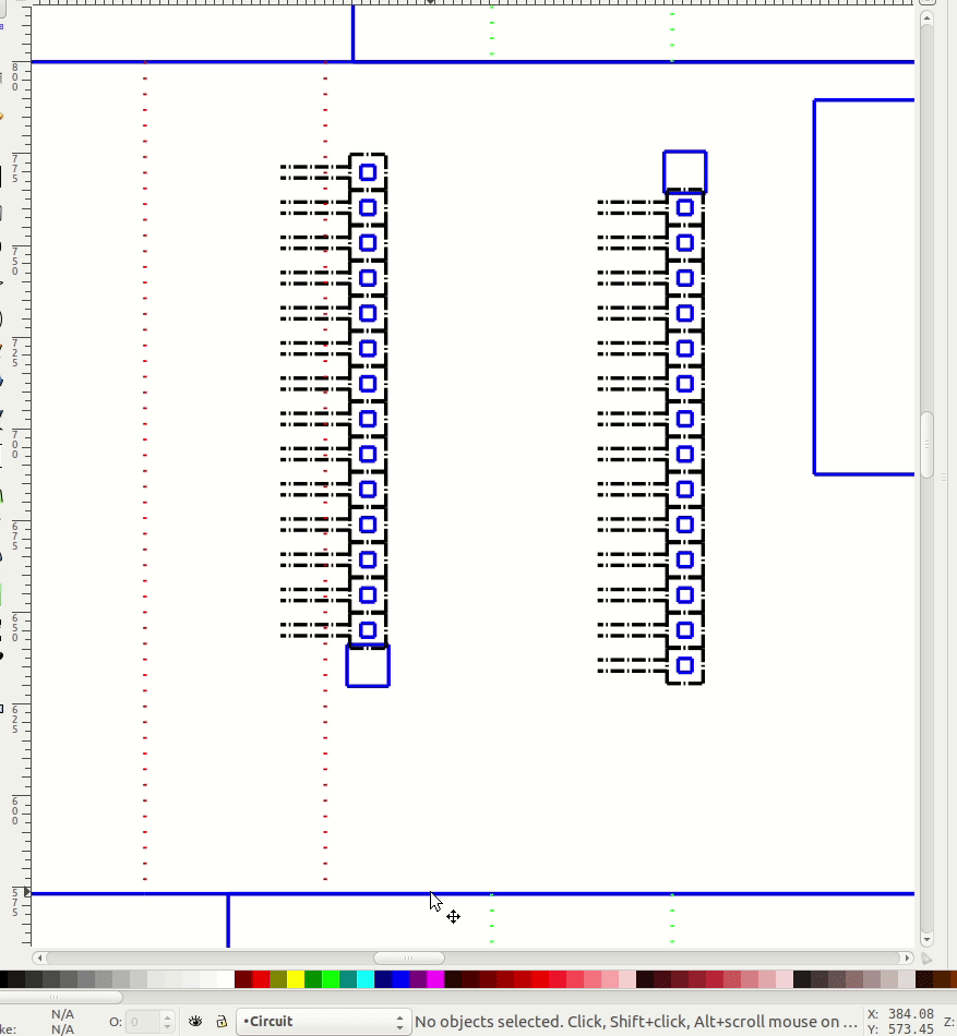
- A script that pulls out pins' coordinate on paper chassis
- Or a image process package (OpenCV) that reads pins' coordinate on paper chassis
- A package solves multi-node path finding problem*
-
Following tasks can be completed by running the code:
- Layers can be cut separately by toggling visibility
- Set cuts with same
intensityandfeedrateon same layer - Able to detect pin center coordinate
- Able to draw arbitrary shape around the pin center
Detecting microcontroller pin center allows the pathfinding package to locate start and end point. It also helps building the circuit. Putting different cuts on separate layers is making the fabrication process easier.